News
Yuxiang Display · Technical guide · Sources checked 26 October 2026
A replacement 128×64 COG LCD needs a match in mechanical fit, electrical connections, controller setup and optical performance. Resolution alone describes the pixel matrix. Compare the controlled drawings and pin assignments before connecting a sample, then validate the display in the finished instrument. Two published Yuxiang drawings show how different the construction can be at the same resolution.
The examples below come from the drawings linked on the ST7567 COG product page and the ST7565R COG product page with a PCB assembly. “A” and “B” are labels used in this comparison, not product model numbers.
| Item shown in the drawing | A: FPC construction, drawing 78 | B: PCB construction, drawing 68 |
|---|---|---|
| Pixel matrix | 128×64 | 128×64 |
| Body width and height, using the indicated boundary | 60 × 45.1 mm, backlight outline marked BL | 79.5 × 64.0 mm, PCB outline |
| Active-area width, marked A.A. | 47.97 mm | 66.53 mm |
| Viewing-area width, marked V.A. | 54.2 mm | 72.0 mm |
| Connection shown | 36-contact FPC | 20-position plated-through-hole row on the PCB |
| Contact or hole pitch | 0.5 mm | 2.54 mm |
Sources: published drawing A and published drawing B, inspected on 26 October 2026. These are published design dimensions, not measurements of delivered samples. The outlines refer to different construction boundaries; the FPC extension, component clearance and installation space require separate checks. The web copies do not establish the latest approved revision for a purchase order.
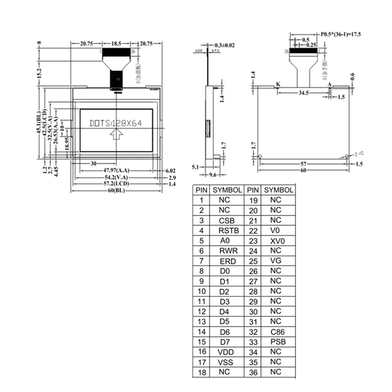
Drawing A includes a pin-assignment table. Obtain the controlled revision before designing the connector or applying power.
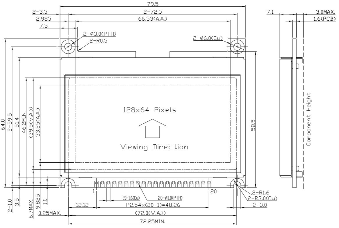
Drawing B shows the mechanical connection layout. This image alone does not provide an electrical assignment for all 20 positions.
The indicated body width differs by 19.5 mm and the height by 18.9 mm, calculated from the dimensions above. A housing designed around A therefore cannot be approved for B from a “128×64” catalogue description. Mounting points, enclosure ribs and the connector need their own comparison.
The distinction between A.A. and V.A. also matters. In drawing A, the marked viewing width is 54.2 mm and the active width is 47.97 mm. The viewing window is wider than the pixel region. Preserve these labels when preparing the bezel drawing or calculating the size of a displayed digit.
Compare the glass, backlight and PCB outlines separately. Mark which surface locates the display in the enclosure. Then check the active-area position relative to that surface, the bezel opening and the connector.
A connector can have the correct pitch and still be unsuitable. Check the contact count, exposed-contact side, insertion direction, FPC thickness and usable insertion length. Route the flex against the permitted bending zone in the approved drawing. Keep mounting pressure and enclosure features away from areas identified as restricted by the supplier.
The two examples above use different connection forms. A 36-contact FPC and a 20-position PCB row require different host connections even though both assemblies display 128×64 pixels. An adapter requires an electrical mapping and a mechanical review.
Create a mapping with four columns: existing display pin, existing function, candidate display pin and required board change. Work from each module's approved pin table, not from a controller name or a photograph.
Drawing A identifies pin 16 as VDD and pin 17 as VSS. Those assignments belong to that drawing. They do not establish the assignments of drawing B or another ST7567 module.
For the electrical review, confirm:
Module supply range and power-on sequence, including reset timing.
Host I/O levels and the controller's input limits. Check any level translation already present on the module PCB.
Interface-selection pins and their required states for the chosen bus.
Connections for contrast or LCD drive generation, including any required external components.
Backlight supply, current control and polarity as a separate circuit.
The product pages identify ST7567 for A and ST7565R for B. Each page lists a 3.3 V operating voltage. These catalogue entries do not establish 5 V tolerant inputs or an identical pinout. Use the electrical specification of the exact assembly and revision.
Firmware reuse depends on the controller variant and the module wiring. Compare the documented reset sequence, bus timing, power-control settings, bias and contrast settings. Check the visible column range, segment/common direction and any addressing offset used by the existing code.
The U8g2 constructor reference lists separate ST7565 and ST7567 families and several module-specific variants. This illustrates why a library selection needs more detail than resolution. A constructor for another manufacturer's display is not evidence that it matches these two assemblies.
Use a test image that reveals mapping errors: an outer pixel border, alternating rows and columns, all pixels on and off, and the actual instrument screens. Check minus signs, decimal points, units and alarm text. A menu that appears correctly can still leave an edge column or an alarm symbol untested.
Keep the existing approved display as a comparison sample. Record the candidate's model, drawing revision, controller information, hardware revision and firmware version. Agree the operating conditions and pass criteria before testing.
Inspect the fit. Check bezel coverage, mounting features, FPC routing and component clearances against the assembly drawing.
Verify the electrical configuration. Check the pin mapping and interface-selection state before powering the sample. Measure the specified supply and reset behavior during startup.
Check display content. Run the pixel patterns and normal measurement, menu and alarm screens. Confirm that values and their signs remain legible.
Exercise power transitions. Test the specified startup, shutdown, sleep, wake and supply-dip conditions. Record recovery behavior against the instrument requirements.
Test the required environment. Evaluate readability, startup and updating at the agreed temperatures and viewing positions. The LCD cold-start test guide separates optical response, contrast and electrical startup faults.
Close the record. Save conditions, instruments used, sample identification, observations and the approval decision. A blank worksheet is a test plan; it becomes evidence only after the actual results are recorded.
Measure display and backlight current in defined operating states if battery life matters. A resolution match does not determine the backlight load or the instrument's runtime.
For a request to Yuxiang Display, provide the existing part number and revision, its drawing and pin table, the available enclosure space, the host interface and I/O voltage, and the required temperature range. Include the display screens or photographs that define readability requirements. State whether PCB changes or a connector adapter are acceptable.
Use the COG display catalogue to identify candidates, then send the requirement and existing documentation. Confirm the proposed assembly's controlled documentation and sample acceptance requirements before treating it as a replacement.
Matching resolution is only the first check. The two published drawings here show different outlines, contact counts and pitches. Approve the mechanical, electrical, firmware and optical requirements of the exact candidate before replacing the existing display.
Reuse needs a comparison of the exact controller documents and module wiring. Review initialization, bus timing, addressing, orientation and contrast settings. A shared resolution or a similar command name does not establish complete compatibility. Verify the result with pixel patterns and the instrument's real screens.
Check the module's input-voltage limits and any level translation in the actual circuit. A 3.3 V operating-voltage entry describes a supply condition; it does not confirm 5 V tolerant inputs. Use level translation where the documented electrical limits require it.
A tightly packed, one-bit-per-pixel full framebuffer needs 128 × 64 ÷ 8 = 1,024 bytes, or 1 KiB. This is a calculated pixel-buffer size. Library state, alignment, additional buffers and application data can require more RAM. A page-buffer implementation uses a different buffering strategy.
A.A. identifies the active pixel area; V.A. identifies the viewing area. Drawing A marks their widths as 47.97 mm and 54.2 mm respectively. Use the supplier's drawing definitions and positions when designing the bezel. The two widths are not interchangeable.
Contact count, pin functions, contact side and connector geometry also need to match. The same pitch can carry a different signal assignment. Compare the complete pin tables before connecting the sample; never infer supply pins from pitch alone.
Define the required temperature, stabilization condition, supply behavior, startup sequence and readable-screen criterion. Test the candidate in the intended instrument configuration and record the outcome. Storage-temperature capability alone does not prove that the assembled instrument will start and display correctly at that temperature.
Request the exact model and controlled drawing revision, electrical pin table, interface and initialization requirements, backlight specification, and applicable operating limits. Link the acceptance record to that configuration. Resolve discrepancies between a catalogue entry and a controlled document before releasing the PCB or purchase order.
Yuxiang ST7565R COG/PCB product page and its linked drawing 68.
U8g2 official project wiki: constructor reference. Used for the existence of controller and module-specific configurations, not as electrical approval for a Yuxiang module.
The source dimensions are transcribed from the indicated drawing labels. Dimensional differences and framebuffer size are calculations. No sample measurements, customer project results or certification test results are claimed in this article.